When configuring a test enclosure with multiple I/O filters and interfaces, it is important to understand how each additional filter affects the overall system isolation. In some cases — particularly when testing devices that use high-order modulation formats such as GPS, modern WiFi (802.11ac/ax/be), or Bluetooth Low Energy — the cumulative effect of multiple I/O paths can reduce system isolation enough to affect your test results. This paper explains the physics, provides the math, and offers practical techniques for mitigating the effect.
The Weakest Link Principle
Every JRE Test enclosure provides a minimum of -100 dB shielding isolation from DC to 1 GHz. But the enclosure itself is only one part of the system. Every I/O filter, connector, and interface installed on the I/O plate has its own isolation specification, and the overall system isolation is determined by the weakest link — not the enclosure.
For example, the JRE USB 2-1 is specified at greater than 80 dB isolation up to 1 GHz. If you install a single USB 2-1 on an enclosure that provides 100 dB of isolation, the system isolation drops to approximately 80 dB — the filter is now the limiting factor, not the enclosure walls. The enclosure’s 100 dB of shielding is still there, but the signal finds an easier path through the filter at 80 dB than through the enclosure walls at 100 dB.
This is not a defect — it is the inherent tradeoff of having any connection cross the shielding barrier. The filter provides excellent isolation while still passing your data signals through. But it means that when evaluating your system’s total isolation, you must look at the I/O configuration, not just the enclosure specification.
The Parallel Leakage Effect: 3 dB Per Doubling
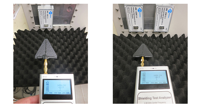
Enclosure shown with one and two JRE USB2-1 filters
What happens when you add a second filter at the same isolation level? The answer follows directly from basic circuit theory. Think of each I/O filter as a resistor in a parallel circuit — each one provides an additional path for RF energy to leak through the enclosure wall. Just as adding a resistor in parallel reduces the total resistance, adding a filter in parallel reduces the total isolation.
When you go from one filter to two identical filters, you have doubled the number of leakage paths, which doubles the total leakage power. A doubling of power equals 3 dB. So if one USB 2-1 filter provides 80 dB of isolation, two USB 2-1 filters in the same enclosure provide approximately 77 dB.
This 3 dB per doubling rule continues as you add more filters:
| Number of I/O Filter Paths | Degradation from Single-Filter Isolation |
| 1 | 0 dB (reference) |
| 2 | 3.0 dB |
| 3 | 4.8 dB |
| 4 | 6.0 dB |
| 5 | 7.0 dB |
| 6 | 7.8 dB |
| 8 | 9.0 dB |
| 10 | 10.0 dB |
| 12 | 10.8 dB |
| 16 | 12.0 dB |
| 24 | 13.8 dB |
| 48 | 16.8 dB |
The math is simply 10 × log₁₀(N), where N is the number of identical filter paths. Even with 48 filters — far more than any typical configuration — the total degradation is under 17 dB. The effect is real but manageable.
An Important Clarification: RF Bulkhead Connectors Are Not Leakage Paths
Unfiltered RF bulkhead connectors — SMA, BNC, Type N, and similar — do not degrade the enclosure’s isolation. The coaxial cable’s shielding is continuous from the external equipment, through the bulkhead connector, and into the chamber. There is no break in shielding, so there is no leakage path. You can install as many RF bulkhead connectors as you need without affecting system isolation.
The degradation table above applies only to filtered I/O interfaces (USB, Ethernet, HDMI, DB connectors, terminal strips, power entry modules) where the filter itself has a finite isolation specification. Unfiltered coaxial feedthroughs do not factor into the calculation.
Typical Filter Isolation Specs
To apply the degradation table to your specific configuration, you need to know the isolation specification of each filter you are installing. Here are the approximate isolation figures for common JRE Test interfaces at 1 GHz (consult each product’s page for full specifications across frequency):
JRE USB 2-1: >80 dB JRE USB 3-1: >60 dB JRE USB-C: >60 dB JRE LAN-1: >80 dB JRE LAN-10G: >60 dB JRE HDMI-1: >60 dB JRE PEM-1 (AC power): >80 dB Filtered DB9 (1000 pF): >60 dB Terminal strip filters (Pi-filter): 60–75 dB
Note that the patented high-speed filters (USB 3, USB-C, LAN-10G, HDMI) typically have lower isolation specifications than the low-pass or capacitive filters (USB 2, LAN-1, DB connectors). This is the inherent tradeoff of passing high-speed data that occupies the same frequency range as the interference — the filter must be more permissive to avoid degrading the data, which means somewhat less RF attenuation.
A Worked Example
Consider a JRE 1714 enclosure (two C-size I/O plates) configured for testing a WiFi access point with the following I/O:
- 1× JRE USB-C filter (>60 dB)
- 1× JRE LAN-1 Ethernet filter (>80 dB)
- 2× SMA bulkhead connectors (not leakage paths — ignore)
- 1× JRE PEM-1 AC power entry (>80 dB)
- 1× 4-terminal DC filter strip (60–75 dB, call it 65 dB)
The system isolation is determined by the weakest filter — in this case, the USB-C at 60 dB. The other filters contribute additional parallel leakage paths, but because they have higher isolation than the USB-C, their contribution to the total leakage is relatively small. The dominant leakage path is the USB-C filter.
To be conservative, treat the four filtered interfaces (USB-C, LAN-1, PEM-1, terminal strip) as four parallel paths at the weakest filter’s specification. From the table, four paths add 6 dB of degradation. So system isolation is approximately 60 – 6 = 54 dB as a worst-case conservative estimate.
In practice, the actual isolation will be better than this because the LAN-1 and PEM-1 are 20 dB better than the USB-C — their leakage contribution is negligible compared to the USB-C. A more realistic estimate would be closer to 58–60 dB, with the USB-C dominating. The conservative calculation gives you a safe lower bound.
For most test scenarios, 54 to 60 dB of system isolation is more than sufficient. But for testing devices with very sensitive receivers — GPS, modern WiFi, BLE — it may not be, which brings us to the next topic.
Why It Matters: Processing Gain and Sensitive Receivers
Early WiFi devices (802.11b) used a relatively simple modulation format, achieving 2 Mbps over a 22 MHz bandwidth. The signal was robust and easy to detect. Modern WiFi (802.11ax, 802.11be), GPS, Bluetooth Low Energy, and many IoT protocols use far more sophisticated modulation — OFDM, spread spectrum, and high-order QAM formats that spread data across wide bandwidths, often with the signal power at any given frequency below the ambient noise floor.
How can these devices operate with signals below the noise? The answer is processing gain — the receiver’s ability to extract a known signal pattern from noise by correlating across a wide bandwidth and over time. A GPS receiver, for example, operates with received signal levels around -130 dBm, far below the thermal noise floor, and uses approximately 43 dB of processing gain to recover the signal. Modern WiFi receivers routinely operate at sensitivity levels of -85 dBm or better.
What this means for your test enclosure is that even modest RF leakage — levels that would be completely negligible for older, simpler devices — can be detected and decoded by modern receivers. A system isolation of 75 dB means a 0 dBm signal outside the enclosure arrives inside at -75 dBm. A WiFi router down the hall at that level is easily detected by a modern WiFi chipset. A GPS signal at -130 dBm outside, arriving at -205 dBm inside after 75 dB of isolation, is well below any receiver’s capability — but a strong nearby WiFi access point or cellular signal at 0 to +20 dBm may not be sufficiently attenuated.
A note on RSSI readings: if your device displays a received signal strength indicator (RSSI) or dBm reading, be aware that many implementations measure only peak power from a small number of data packets rather than averaging over a long period. The RSSI reading is useful as a quick indicator that a signal is present, but it is not a precise measurement of the continuous RF power environment your device is experiencing. Do not rely on RSSI alone to assess whether your enclosure isolation is adequate.
Practical Techniques for Improving System Isolation
If your test results suggest that leakage through the I/O filters is affecting your measurements, here are proven techniques to improve the situation:
Minimize the number of active I/O connections. The I/O plate system is designed for exactly this purpose — rather than populating a single plate with every conceivable connector, configure the plate with only the interfaces you need for the current test. Swap in a different plate when your test requirements change. Unused filtered connectors that are installed but not connected to external cables are less of a concern, but an empty plate with fewer penetrations is always better.
Use high-quality shielded cables on the external side. The external cable connected to each I/O filter acts as an antenna — it picks up ambient RF from the environment and conducts it to the filter, which then must attenuate it. A better-shielded cable picks up less ambient RF in the first place, reducing the signal the filter has to reject. In our testing, switching from an unshielded Cat 5 Ethernet cable to a shielded Cat 7 cable improved system isolation by over 10 dB.
Pay attention to external cable routing. Moving an I/O cable just a few centimeters — away from other cables, away from nearby RF sources, or closer to the enclosure body — can improve isolation measurably. At GHz frequencies, small changes in cable position change the antenna coupling significantly.
Add absorber foam near the I/O plate inside the enclosure. This is one of the most effective and easiest techniques. Placing a piece of RF absorbing foam inside the enclosure near the I/O plate attenuates any signal that leaks through the filters before it can propagate to the device under test. In our measurements, simply setting a loose piece of absorber foam against the inside of the I/O plate reduced leakage by over 10 dB.
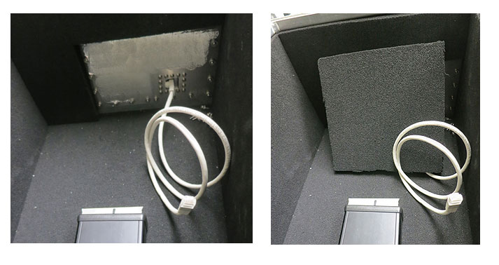
Inside view: without foam (left) and with foam placed against I/O plate (right)
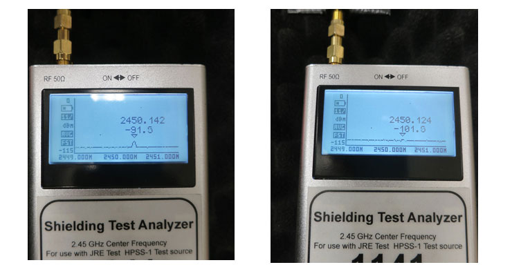
Spectrum analyzer display: signal leakage without foam (left) and with foam (right) — over 10 dB improvement
Contact us if you need additional absorber foam pieces for this purpose.
Consider fiber optic connections where maximum isolation is required. Fiber feedthrough connectors provide complete electrical isolation — no conducted RF path at all. If one particular I/O connection is the dominant leakage path and the application allows fiber, switching that connection to fiber eliminates it from the leakage budget entirely.
The Art and the Engineering
Reducing leakage and improving system isolation at GHz frequencies is sometimes more art than calculation. When you are dealing with receivers capable of operating at -85 dBm or lower, and your isolation budget is measured in factors of hundreds of millions (80 dB = 100,000,000:1 power ratio), every detail matters — cable position, shielding quality, connector torque, foam placement, even the orientation of the device inside the chamber. The good news is that the techniques described above are effective, inexpensive, and easy to implement. A combination of careful I/O selection, good cables, and a piece of absorber foam near the I/O plate will handle the vast majority of situations.
Further Reading
For guidance on selecting an enclosure and choosing I/O interfaces: How to Select and Configure an RF Shielded Test Enclosure.
For the technical details of how each filtering approach works: Understanding Data Signals Through Filtered I/O Connectors.
For measuring and verifying your enclosure’s actual isolation: Measuring and Verifying the Shielding Isolation of an RF Shielded Test Enclosure.
For all available I/O interfaces and their specifications: I/O Interfaces.
If you have questions about how a specific configuration will affect your system isolation, contact us — we can walk through the calculation with you.